


商品の詳細
初めにご覧いただきありがとうございます✨
複数購入してくれる方には値引き頑張ります!!
購入したい金額を提示してくれると助かります✨
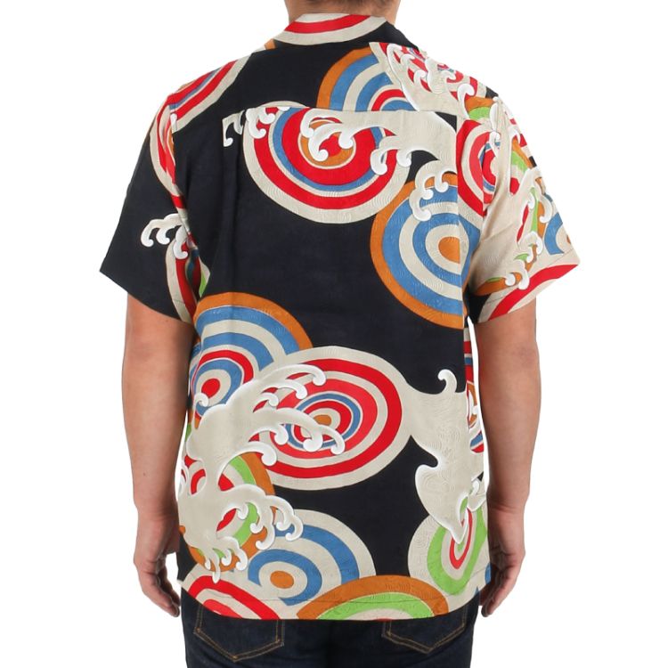
●アイテム
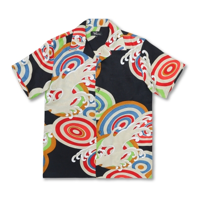
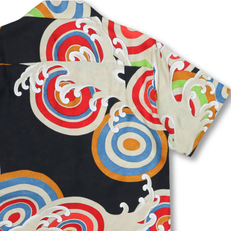
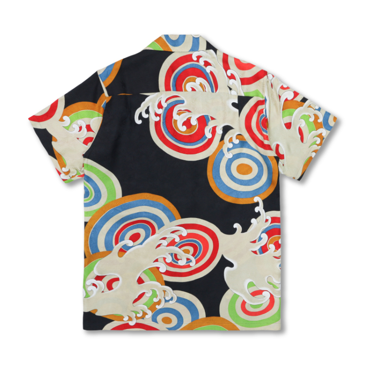
Pagongパゴン
ビンテージヴィンテージ
シルク100%アロハシャツ
渦 立波 赤 和柄 荒波 流水 水しぶき
とても希少なパゴンのアロハシャツいかがでしょうか??
●サイズ L
着丈70cm
肩幅46cm
身幅58cm
素人採寸ですので誤差はご了承ください
●素材
シルク100%
●カラー
レッド
●状態
ヴィンテージ品としては目立つ汚れなどはなく美品部類に入ると思います。
●配送
1〜2日程度での配送を心がけています。
仕事の都合上遅れる可能性がありますので
ご了承ください。
シャツ種類···アロハシャツ
カラー···レッド
袖丈···半袖
柄・デザイン···総柄
襟···オープンカラー(開襟)
素材···絹(シルク)
季節感···春、夏、秋、冬
複数購入してくれる方には値引き頑張ります!!
購入したい金額を提示してくれると助かります✨
●アイテム
Pagongパゴン
ビンテージヴィンテージ
シルク100%アロハシャツ
渦 立波 赤 和柄 荒波 流水 水しぶき
とても希少なパゴンのアロハシャツいかがでしょうか??
●サイズ L
着丈70cm
肩幅46cm
身幅58cm
素人採寸ですので誤差はご了承ください
●素材
シルク100%
●カラー
レッド
●状態
ヴィンテージ品としては目立つ汚れなどはなく美品部類に入ると思います。
●配送
1〜2日程度での配送を心がけています。
仕事の都合上遅れる可能性がありますので
ご了承ください。
シャツ種類···アロハシャツ
カラー···レッド
袖丈···半袖
柄・デザイン···総柄
襟···オープンカラー(開襟)
素材···絹(シルク)
季節感···春、夏、秋、冬
商品の説明

極希少】Pagong パゴン シルク100%アロハシャツ 渦 立波 赤 L-

極希少】Pagong パゴン シルク100%アロハシャツ 渦 立波 赤 L-

極希少】Pagong パゴン シルク100%アロハシャツ 渦 立波 赤 L-

極希少】Pagong パゴン シルク100%アロハシャツ 渦 立波 赤 L 店販用 ...

極希少】Pagong パゴン シルク100%アロハシャツ 渦 立波 赤 L-

極希少】Pagong パゴン シルク100%アロハシャツ 渦 立波 赤 L 店販用 ...
和柄 京友禅アロハシャツ <渦と立波/黒> Pagong メンズ - パゴン

pagongのシルク100%アロハシャツ 鶴赤 - fourthquadrant.in
和柄 京友禅アロハシャツ <渦と立波/黒>

極希少】Pagong パゴン シルク100%アロハシャツ 渦 立波 赤 L 店販用 ...

約100年の伝統からなる「京友禅アロハシャツ」100%シルクの着心地と ...
花柄 京友禅アロハシャツ <菊/黒赤>
和柄 京友禅アロハシャツ <渦と立波/黒>
和柄 京友禅アロハシャツ <渦と立波/黒> Pagong メンズ | 京友禅 ...
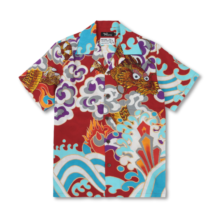
歌舞伎柄 京友禅アロハシャツ <意休の龍/赤>
メンズ・トップス・シャツのデイリーランキング
-
-
5

コモリ comoli 5pデニム サイズ1
デニム/ジーンズ
¥11,825


![Solo Pierce】[セカンドピアス]K18ミッキーマウス☆ハーフピアス](https://static.mercdn.net/item/detail/orig/photos/m41964690986_1.jpg)
